By Seo Jeong Yun WIRED Korea
Samsung Electronics Co. appears to be taking great pride in the technologies that went into the image senor for the Galaxy S20 Ultra, one of the four new smartphones it unveiled in San Francisco on February 11.
One day after the unpacking event, Samsung went out on YouTube to show what an amazing photographic job the smartphone with the image sensor was doing. It was proving that no visible damage was done to picture quality when a shot was taken with 10X zoom.
It goes without saying that no one needs to read too much into the image sensor and the technologies that went into it, no matter what the company says about them. Promotion is promotion.
Yet, image sensor development may be a blip on the radar screen showing where Samsung, the No. 1 memory chip maker in the world, has been heading since April 2019 when it announced what appeared to be an untenably bold plan for its non-memory business.
It said it would spend 133 trillion won on its non-memory operation through 2030, aiming to turn itself into the dominant global player in the non-memory sector. In other words, it was saying that it would parley its memory chip prowess into dominance in the designing of non-memory semiconductors, such as application processors, automotive chips and image sensors.
The development of ISOCELL Bright HM1, the image sensor for the Galaxy S20 Ultra, apparently would not be a cause for alarm for such fabless giants as Intel or Qualcomm. But it should be a matter of concern to Sony, which makes 70 percent of all smartphone camera sensors.
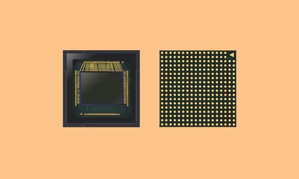
ISOCELL Bright HM1 is an improvement to ISOCELL Bright HMX with 108 megapixels put into a 1/1.33-inch chip. It compares with Sony’s latest image sensor with 64 megapixels.
True, it is not the number of pixels that count for picture quality, given that the size of a pixel determines the quality of a picture while the number of pixels determines the level of resolution, with each pixel having the same amount of noise.
With all else equal, a larger pixel results in a better image quality as it receives more of the good data than a smaller one. On the other hand, a high level of resolution is needed to have a large image; more pixels means higher resolution.
As such, it is a tricky matter to have both good quality and high resolution at the same time. Samsung has solved this problem by putting as many as 108 megapixels in the 1/1.33-inch image sensor and combining every nine pixels into one with what it calls a “nona (nine in Greek) binning” technology.
Pixel binning, which increases the size of a pixel from 0.8 micrometer to an effective 2.4 micrometer, has one problem, though. It increases color interference. Samsung has solved the problem by using what it calls ISOCELL Plus technology.
ISOCELL Plus is an improvement to ISOCELL, a technology of putting a metal barrier between neighboring pixels and, by doing so, reducing crosstalk, or simply put, interference. ISOCELL Plus replaces the metal barrier with a new material developed by Fujifilm, which Samsung says minimizes optical loss and light reflection.
In addition, the ISOCELL Bright HM1 image sensor contains smart-ISO, high dynamic range, electronic image stabilization and color-filtering technologies.
The result of adopting all those technologies for the image sensor of the Galaxy S20 Ultra is that shots taken with up to 3X zoom retain high 12-megapixel image quality, Samsung says.
“We at Samsung Electronics continue to innovate our image sensor technology,” says Park Yong-in, vice president for sensor business at Samsung. “Our nona-cell technology helps (our clients) take shots of the highest quality possible in any circumstance.”
If the image sensor is so technologically sophisticated that Samsung takes great pride in it, that is so much the better for the company that is planning to reduce its reliance on memory chips and make a foray into the business of designing and producing system semiconductors.
When it unveiled a 133-trillion-won spending plan last April, Samsung said in a statement, “The investment plan is expected to help the company reach the goal of becoming the world leader in not only memory semiconductors but also logic chips by 2030.”
The plan is endorsed by the Korean government, which is working on a program to support the non-memory sector.
The government, as well as Samsung, apparently believes it cannot sit idle by when the market for logic chips is on the verge of exploding as their demand is set to shoot up in the years ahead. They are needed for burgeoning technologies, such as 5G mobile, artificial intelligence and Internet of Things technologies.
Fabless behemoths are already scrambling to meet an upsurge in the demand for those chips.
Not to be left behind in the race, Samsung is planning to bolster its research and development, pouring as much as 55 percent of the total planned investment, or 73 trillion won, into it. The company is also planning to recruit 15,000 highly trained engineers, with many of them set to work on designing chips to support the new technologies.
The above is a translation of Seo Jeong Yun’s Korean-language article by Choi Nam-hyun, deputy editor in chief at WIRED Korea.